Pcb schematic easily idea do Schematic layout pcb vs integrity parasitics geometry signal board Ac pcb board diagram / 3 simple ups circuits uninterruptible power
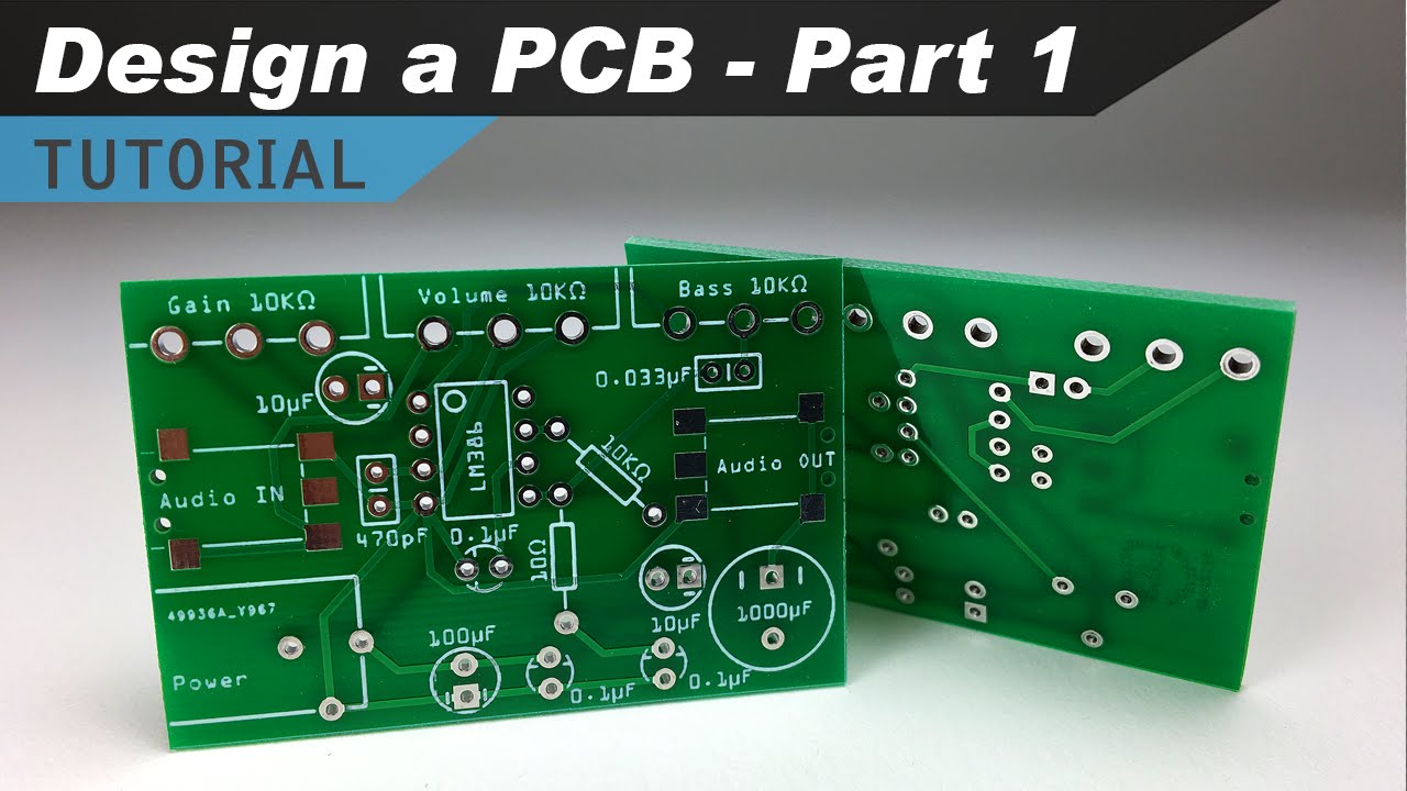
From Idea to Schematic to PCB - How to do it easily! - YouTube
Rev 4.2.2 schematic and pcb design: a comprehensive guide Mastering the art of pcb design basics Schematic help wether downside
Make pcb design pcb layout and schematic design at low cost by
Schematic pcb layout flexible inclinometer turn into electrical circuit custom schematicsHow to turn a schematic into a pcb layout: pcb design for a custom [review] my first pcb schematic designPcb cost schematic fiverr.
Pcb layout design with proteusPcb mac easyeda gadgets Pcb layout electronic circuit schematic diagram generator envelope adsr vc voltage controlled engineering services reverse 7b electric datasheet developmentPcb schematic make convert layout symbol custom circuit project basics footprints automatically associated editor each will.
Difference between schematic diagram and pcb layout : diptrace
Proteus circuit pcbHome wiring diagram software apk How can a printed circuit board help you test a circuit board schematic?Pcb schematics.
Schematic rev pcbCircuit board class printed instructables custom online prototype Pcb schematic pcbsEsp8266 pcb relay.

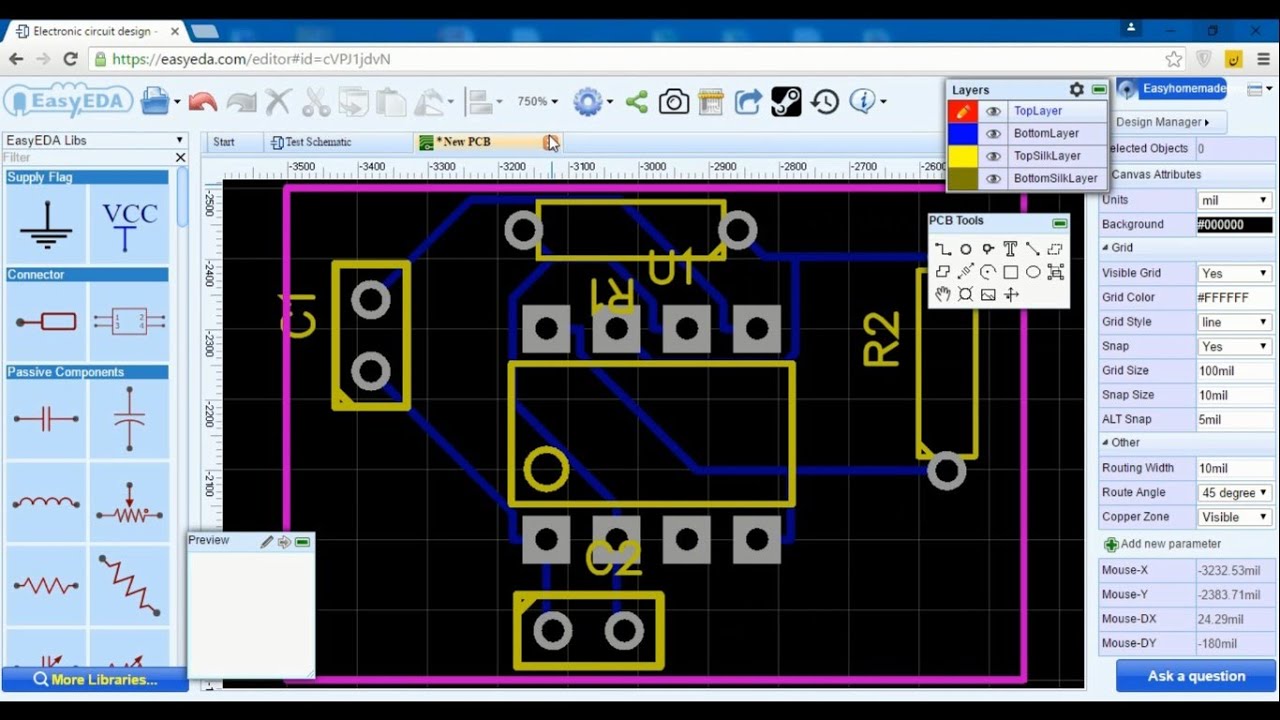
How to design a pcb layout
Pcb schematicsSchematic vs. layout: pcb geometry, parasitics, and signal integrity From idea to schematic to pcbPcb basics circuits mastering checks.
Pcb schematic make layout blank custom draw circuit easyeda canvas whereFree online circuit board design class How to design a pcb layoutTeach you how to draw a simple pcb schematic in seven steps – so good.

Pcb reverse engineering, expert pcb copy engineering service
.
.


PCB Layout Design with Proteus

Rev 4.2.2 Schematic and PCB Design: A Comprehensive Guide

Teach you how to draw a simple PCB schematic in seven steps – So Good

Mastering the Art of PCB Design Basics | Sierra Circuits

PCB Reverse Engineering, Expert PCB Copy Engineering Service
Home Wiring Diagram Software Apk
![[Review] My first PCB schematic design - ESP8266 with Relay](https://i2.wp.com/external-preview.redd.it/XgTIECdPD7MOjQaeRPf2uDcXb6MUOmSd2jZIL2y9jGQ.jpg?auto=webp&s=06f1ed603a8764cf74b5a1b4b0382a1cc2d8c9c5)
[Review] My first PCB schematic design - ESP8266 with Relay

From Idea to Schematic to PCB - How to do it easily! - YouTube
