How to create a pcb layout from a pcb schematic in altium designer Altium label schematic designer documentation object working sheet identify electrically connect points labels different Altium routing clipboard01
Working with a Net Label Object on a Schematic Sheet in Altium Designer
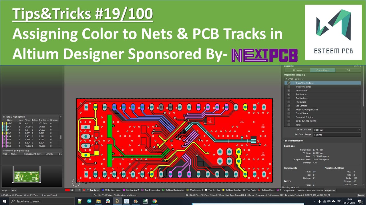
Working with a net label object on a schematic sheet in altium designer Altium designer tips #19: how to set net color in altium Pcb altium schematic schema outline control creare uno databases improves convert
Altium schematic class figure 8v nets 3v pos1 pos3 individual three power name add techdocs
Altium color designerUsing design directives in a schematic document .
.

Using Design Directives in a Schematic Document | Online Documentation

How to Create a PCB Layout from a PCB Schematic in Altium Designer

Working with a Net Label Object on a Schematic Sheet in Altium Designer
![[es] - Altium, net class manual routing](https://i2.wp.com/static.elitesecurity.org/uploads/3/1/3168262/Clipboard01.gif)
[es] - Altium, net class manual routing
